Laying out a PCB for an ATmega32u4 based board
Feb 26, 2023: While this information is still accurate I would never, ever, do an ATmega32u4 PCB anymore. Instead I use an RP2040 chip. So much easier to find, cheaper, and easier to deal with.
It’s one thing to design a nice schematic for a board based on an ATmega32u4. It’s quite another to figure out how to get all the traces to work well on the actual PCB you’re planning to send off to fabrication.
In this post, part 2 in a series, I’ll walk through some of the things that worked for me when trying to solve layout issues during my custom PCB design.
Routing the power traces
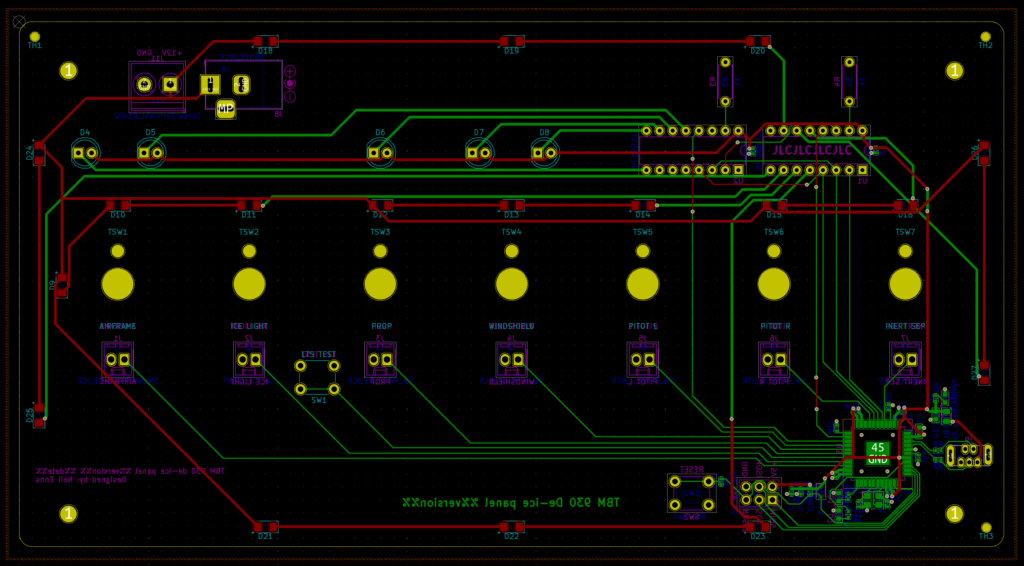
For cost reasons I really wanted to keep this to a 2-layer board which meant I couldn’t fall back to a dedicated power plane on an inner board layer. I’ve done PCBs in the past and routing the power traces was pretty easy but dealing with the ATmega32u4 was… tricky.
Package selection makes a difference here. Originally I tried to use a QFN package but those pins are tiny and I was really having a tough go of it. Things got a lot easier when I switched to TQFP, which conveniently is easier to hand solder as well.
The other trick is to remember you can run traces underneath the chip (something I always forget). To get all the VCC pins connected I took full advantage of this, running all the power traces on the front side of the board and using vias to pop them out on the back side where the 32u4 lived:
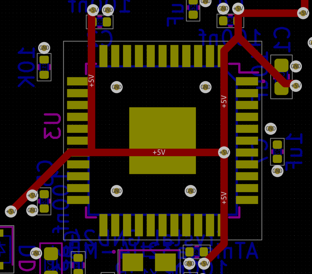
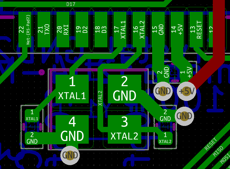
Placing the decoupling capacitors and oscillator
The capacitors and oscillator should be placed as close to the ATmega32u4 as possible. I tried several layouts and what worked for me was to use teeny tiny capacitors (0402) placed close to the power and ground pins, but still leaving enough space to get a soldering iron in since I was going to hand solder the 32u4. Since I planned to use JLCPCB’s SMT assembly service for all the small components on the back of the board I thankfully didn’t have to worry about trying to solder the tiny capacitors.
The oscillator and its associated capacitors also took a bit of layout tweaking but eventually I settled on this:
The other thing that helped me with this part of the layout was to route all the power traces first.
Routing the data lines
The data lines coming off the GPIO pins were something I redid multiple times. My initial pin assignment in the schematic for each of the data lines was essentially arbitrary and many of them just didn’t make sense when it came to doing the board layout. I kept hitting situations where I was jumping traces between board layers and the overall trace layout was messy.
This is where going back to the schematic and making changes is valuable. There are only two lines that have to be on pins with PWM support (the two that control LED brightness). All the other data lines can go on any GOIP pin.
I did several revisions where I swapped data lines to different pins, doing my best to select pins that were closer to where the traces eventually had to run. Don’t be afraid to revise your schematic! In the end I came up with this:
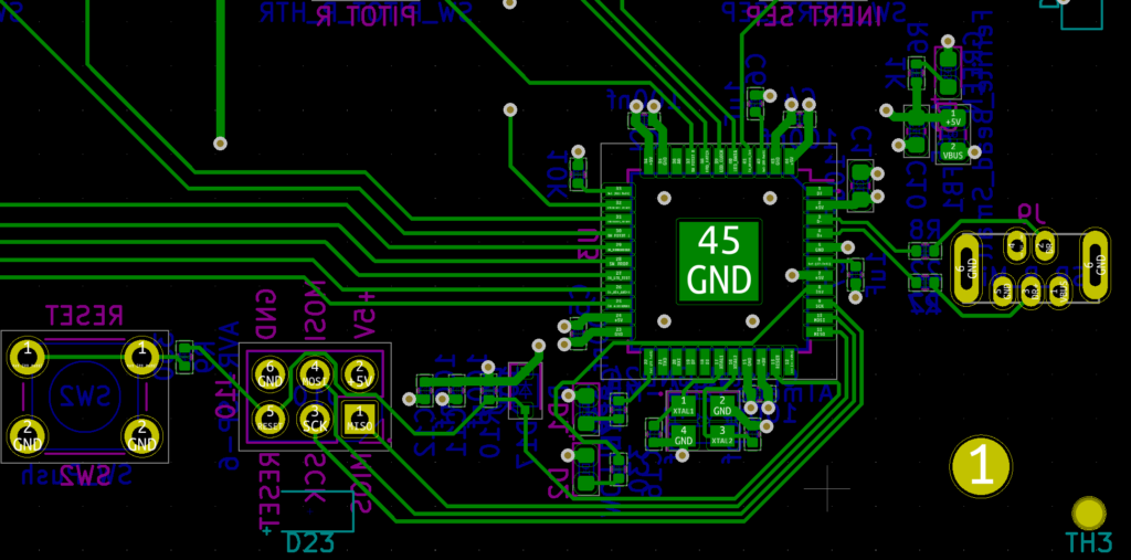
The traces are clean, flow reasonably directly to where they need to go, and only a handful of vias were required to jump over other traces.